- 您现在的位置:买卖IC网 > Sheet目录1997 > ICS841602AGILF (IDT, Integrated Device Technology Inc)IC CLOCK GENERATOR 28-TSSOP
IDT / ICS HCSL CLOCK GENERATOR
13
ICS841602AGI REV. A JULY 10, 2008
ICS841602I
FEMTOCLOCKS CRYSTAL-TO-HCSL CLOCK GENERATOR
3. Calculations and Equations.
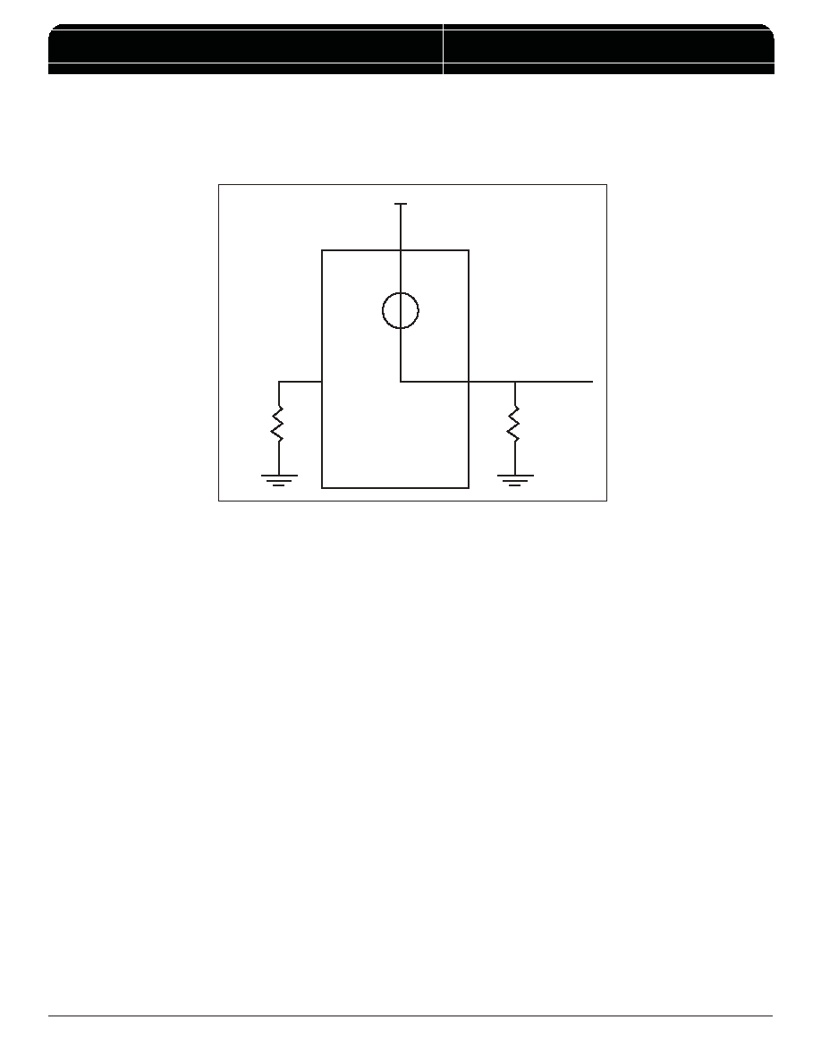
The purpose of this section is to calculate power dissipation on the IC per HCSL output pair.
HCSL output driver circuit and termination are shown in
Figure 6.
HCSL is a current steering output which sources a maximum of 17mA of current per output. To calculate worst case on-chip power
dissipation, use the following equations which assume a 50
Ω load to ground.
The highest power dissipation occurs when V
DD is HIGH.
Power
= (V
DD_HIGH – VOUT
) * I
OUT,
since V
OUT
= I
OUT
* R
L
= (V
DD_HIGH – IOUT
* R
L) * IOUT
= (3.465V – 17mA * 50
Ω) * 17mA
Total Power Dissipation per output pair = 44.5mW
FIGURE 6. HCSL DRIVER CIRCUIT AND TERMINATION
VDD
VOUT
RL
50
Ω
IC
IOUT = 17mA
RREF =
475
Ω ± 1%
发布紧急采购,3分钟左右您将得到回复。
相关PDF资料
ICS841608AKI
IC CLOCK GENERATOR 32-VFQFPN
ICS841S012DKILF
IC FREQ SYNTHESIZER 56VFQFN
ICS842023BGLF
IC CLK GEN ETHERNET 25MHZ 8TSSOP
ICS8421002AGILF
IC FREQ SYNTHESIZER 20-TSSOP
ICS8422002AGILF
IC SYNTHESIZER LVHSTL 20-TSSOP
ICS8427DY-02LF
IC SYNTHESIZER 500MHZ 32-LQFP
ICS843001AG-123LF
IC SYNTHESIZER LVPECL 8-TSSOP
ICS843001AG-21LFT
IC SYNTHESIZER LVPECL 24-TSSOP
相关代理商/技术参数
ICS841602AGILFT
功能描述:IC CLOCK GENERATOR 28-TSSOP RoHS:是 类别:集成电路 (IC) >> 时钟/计时 - 时钟发生器,PLL,频率合成器 系列:HiPerClockS™, FemtoClock™ 标准包装:1,000 系列:- 类型:时钟/频率合成器,扇出分配 PLL:- 输入:- 输出:- 电路数:- 比率 - 输入:输出:- 差分 - 输入:输出:- 频率 - 最大:- 除法器/乘法器:- 电源电压:- 工作温度:- 安装类型:表面贴装 封装/外壳:56-VFQFN 裸露焊盘 供应商设备封装:56-VFQFP-EP(8x8) 包装:带卷 (TR) 其它名称:844S012AKI-01LFT
ICS841604AGILF
功能描述:IC CLOCK GENERATOR 28-TSSOP RoHS:是 类别:集成电路 (IC) >> 时钟/计时 - 时钟发生器,PLL,频率合成器 系列:HiPerClockS™, FemtoClock™ 标准包装:2,000 系列:- 类型:PLL 频率合成器 PLL:是 输入:晶体 输出:时钟 电路数:1 比率 - 输入:输出:1:1 差分 - 输入:输出:无/无 频率 - 最大:1GHz 除法器/乘法器:是/无 电源电压:4.5 V ~ 5.5 V 工作温度:-20°C ~ 85°C 安装类型:表面贴装 封装/外壳:16-LSSOP(0.175",4.40mm 宽) 供应商设备封装:16-SSOP 包装:带卷 (TR) 其它名称:NJW1504V-TE1-NDNJW1504V-TE1TR
ICS841604AGILFT
功能描述:IC CLOCK GENERATOR 28-TSSOP RoHS:是 类别:集成电路 (IC) >> 时钟/计时 - 时钟发生器,PLL,频率合成器 系列:HiPerClockS™, FemtoClock™ 标准包装:1,000 系列:- 类型:时钟/频率合成器,扇出分配 PLL:- 输入:- 输出:- 电路数:- 比率 - 输入:输出:- 差分 - 输入:输出:- 频率 - 最大:- 除法器/乘法器:- 电源电压:- 工作温度:- 安装类型:表面贴装 封装/外壳:56-VFQFN 裸露焊盘 供应商设备封装:56-VFQFP-EP(8x8) 包装:带卷 (TR) 其它名称:844S012AKI-01LFT
ICS841608AKI
功能描述:IC CLOCK GENERATOR 32-VFQFPN RoHS:否 类别:集成电路 (IC) >> 时钟/计时 - 时钟发生器,PLL,频率合成器 系列:HiPerClockS™, FemtoClock™ 标准包装:1,000 系列:- 类型:时钟/频率合成器,扇出分配 PLL:- 输入:- 输出:- 电路数:- 比率 - 输入:输出:- 差分 - 输入:输出:- 频率 - 最大:- 除法器/乘法器:- 电源电压:- 工作温度:- 安装类型:表面贴装 封装/外壳:56-VFQFN 裸露焊盘 供应商设备封装:56-VFQFP-EP(8x8) 包装:带卷 (TR) 其它名称:844S012AKI-01LFT
ICS841608AKILF
功能描述:IC CLOCK GENERATOR 32VFQFPN RoHS:是 类别:集成电路 (IC) >> 时钟/计时 - 时钟发生器,PLL,频率合成器 系列:HiPerClockS™, FemtoClock™ 标准包装:2,000 系列:- 类型:PLL 频率合成器 PLL:是 输入:晶体 输出:时钟 电路数:1 比率 - 输入:输出:1:1 差分 - 输入:输出:无/无 频率 - 最大:1GHz 除法器/乘法器:是/无 电源电压:4.5 V ~ 5.5 V 工作温度:-20°C ~ 85°C 安装类型:表面贴装 封装/外壳:16-LSSOP(0.175",4.40mm 宽) 供应商设备封装:16-SSOP 包装:带卷 (TR) 其它名称:NJW1504V-TE1-NDNJW1504V-TE1TR
ICS841608AKILFT
功能描述:IC CLOCK GENERATOR 32-VFQFPN RoHS:是 类别:集成电路 (IC) >> 时钟/计时 - 时钟发生器,PLL,频率合成器 系列:HiPerClockS™, FemtoClock™ 标准包装:1,000 系列:- 类型:时钟/频率合成器,扇出分配 PLL:- 输入:- 输出:- 电路数:- 比率 - 输入:输出:- 差分 - 输入:输出:- 频率 - 最大:- 除法器/乘法器:- 电源电压:- 工作温度:- 安装类型:表面贴装 封装/外壳:56-VFQFN 裸露焊盘 供应商设备封装:56-VFQFP-EP(8x8) 包装:带卷 (TR) 其它名称:844S012AKI-01LFT
ICS841608AKIT
功能描述:IC CLOCK GENERATOR 32-VFQFPN RoHS:否 类别:集成电路 (IC) >> 时钟/计时 - 时钟发生器,PLL,频率合成器 系列:HiPerClockS™, FemtoClock™ 标准包装:1,000 系列:- 类型:时钟/频率合成器,扇出分配 PLL:- 输入:- 输出:- 电路数:- 比率 - 输入:输出:- 差分 - 输入:输出:- 频率 - 最大:- 除法器/乘法器:- 电源电压:- 工作温度:- 安装类型:表面贴装 封装/外壳:56-VFQFN 裸露焊盘 供应商设备封装:56-VFQFP-EP(8x8) 包装:带卷 (TR) 其它名称:844S012AKI-01LFT
ICS841608I
制造商:IDT 制造商全称:Integrated Device Technology 功能描述:FEMTOCLOCKS CRYSTAL-TO-HCSL CLOCK GENERATOR VCO: 500MHz